Process Monitoring System is a function of measuring wafer’s temperature on the irradiated surface during the laser annealing process in real time. It is useful not only for process monitoring but also for reducing the cost of equipment management and tracing when a fault occurs.
SOLUTION
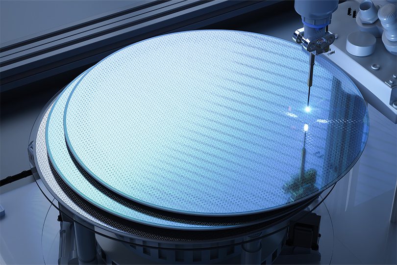
Laser Annealing
Offering real-time water surface monitoring and stable quality control for wafer surface during the manufacturing of power semiconductors
Customers’ issues
- Detection of defects at an early stage to reduce the outflow of defective products.
- Reinforcing traceability
- Improving quality stability
What has been resolved and what can be resolved
Improvement of traceability and quality stability with Process Monitoring System quality.
Monitoring the surface of wafers during laser annealing process makes it easy to discover and identify abnormalities during processing, thereby enabling reinforced process monitoring and tracing. Using this function will save time and reduce the cost of equipment management.
Background of the need for Process Monitoring System during the manufacturing of power semiconductors
In November 2021, the 27th United Nations Climate Change Conference (COP26) was convened, showing the international move to accelerate initiatives for establishing a decarbonized society, as seen in the declaration of carbon neutrality made by many countries.
Power semiconductors are called as the key devices for building a decarbonized society, and their market continues to expand. The performance and productivity of devices are becoming higher and higher, while users are increasingly demanding a high level of quality stability, process management and management of semiconductor manufacturing equipment. There are calls for highly stable quality especially in the category of in-car applications, which drive the growth of power semiconductors.
Process Monitoring System is a function developed to meet customers’ call for enhanced quality control, measuring wafer’s temperature on the irradiation surface during laser annealing process. The function can be used not only for process monitoring but also for reducing the cost of equipment management and tracing when a defect occurs.
Principle of Process Monitoring System that measure thermal radiance of the surface of a heated wafer
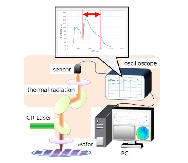
Heating an object causes a phenomenon called thermal radiation, emitting light (electromagnetic wave).
A wafer heated by laser is no exception. The irradiated area becomes hot and starts emitting light in the intensity that depends on the temperature. This light is called thermal radiance. Process Monitoring System is the function of measuring thermal radiance at irradiated areas. Process Monitoring System obtains information associated with the temperature on wafer surface in real time with no physical contact. Measuring results record temperature mapping and average for each of the wafers.
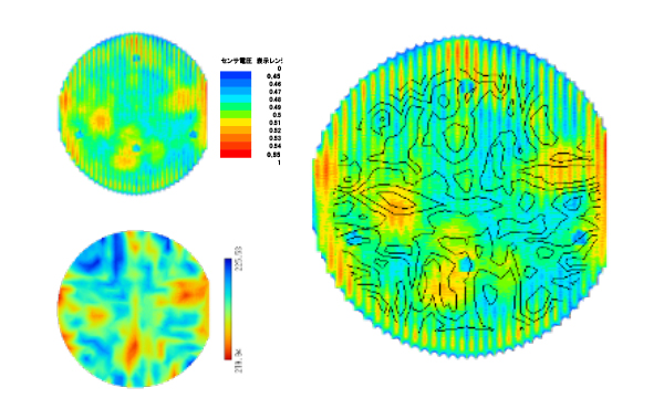
When the results of process monitoring are compared against actually-measured sheet resistance figures, they show a perfect match. Process Monitoring System has high measuring sensitivity, and can substitute sheet resistance measurement to evaluate surface variability and variability between works.
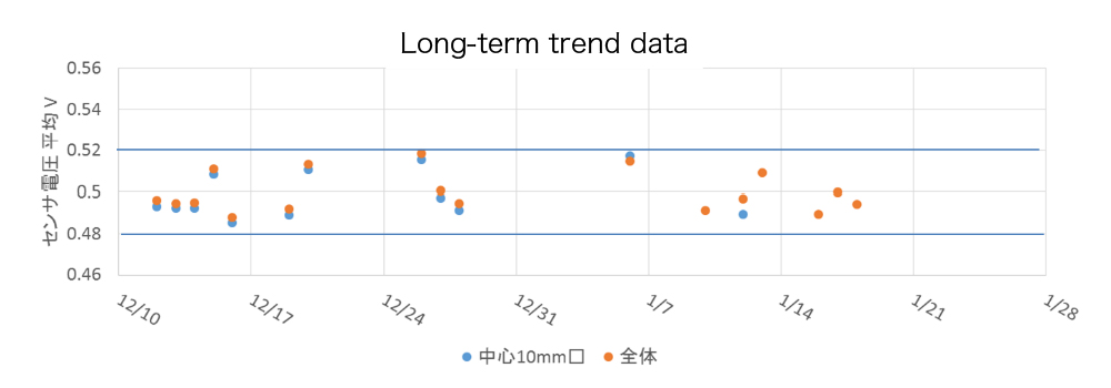
Reducing the cost of equipment management due to Process Monitoring System
Day-to-day equipent management is the key to stable production. Process Monitoring System can be used also for device management. It measures thermal radiance from irradiation on bare wafers for device management, and compares the results with pre-defined thresholds to identify any device fault with ease.
This evaluation is carried out with bare wafers, which can be used repeatedly as long as the heat does not melt them. This reduces costs required for equipment management.
Tracing at the time of fault defect and improving the manufacturing process for power semiconductor devices
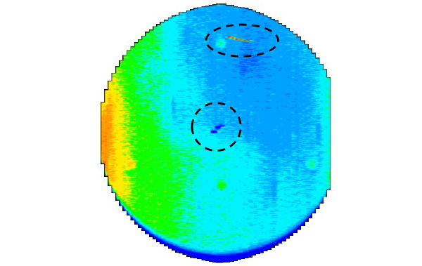
Process Monitoring System measures thermal radiance and produces significant variations in measurement strength when a wafer surface has scratches or foreign matter.
The function can easily identify a wafer with fault and its location, enabling early tracing of defect on manufactured devices.
The mapped shape of a defect location also allows users to estimate defect factors, and use the findings to improve the process, which enables you to explore recurrence-prevention measures.
Stable quality control with Process Monitoring System of Laser Annealing System
The power semiconductor market continues to grow, and there is an anticipated call for higher quality in not only in-car but also in consumer- and industrial applications. Sumitomo Heavy Industries’ Laser Annealing System can meet such calls with the use of Process Monitoring System.
Click here for any queries on process monitoring.
Strengths of Sumitomo Heavy Industries
- Strong track records in manufacturing power semiconductors, resulting in technological maturity and strong reliability
- Capable of supporting from the consideration stage with sample processing and temperature simulation
- Use of proprietary technologies for localized heating
Download a PDF about the 非公開: Product brochure (laser annealing)
Download