PRODUCTS
SWA “UV” Laser series
Laser annealing equipment
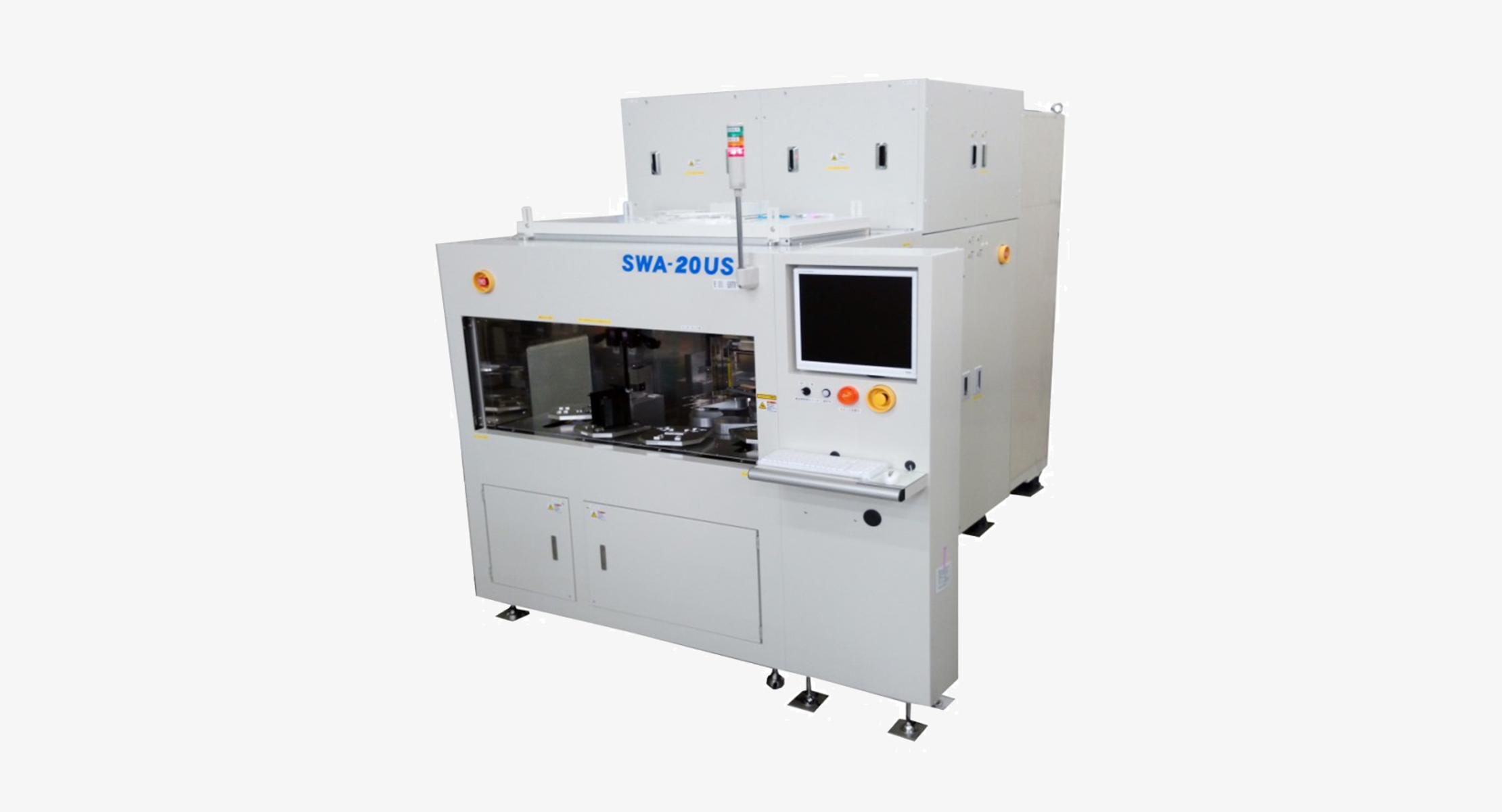
Laser annealing equipment for next generation power devices
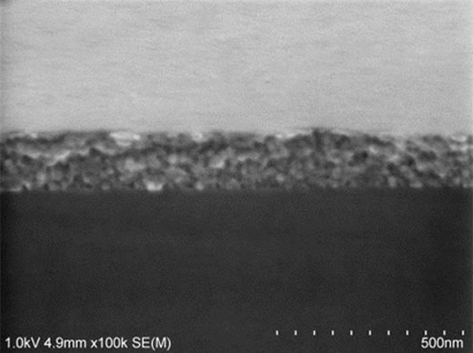
Application example) SiC ohmic contact generation, activation, etc.
The metal-SiC interface is heated to a high temperature while suppressing the temperature rise of the non-irradiated surface, and ohmic contact is created using OPTSWING* (a unique high-speed scanning method).
Application example) SiC ohmic contact generation, activation, etc.
The metal-SiC interface is heated to a high temperature while suppressing the temperature rise of the non-irradiated surface, and ohmic contact is created using OPTSWING* (a unique high-speed scanning method).
Features
High-speed scanning using OPTSWING
Achieves high throughput by scanning the beam.
Compatible with 8 inch wafers
Capable of processing wafers from small pieces to 8 inches.
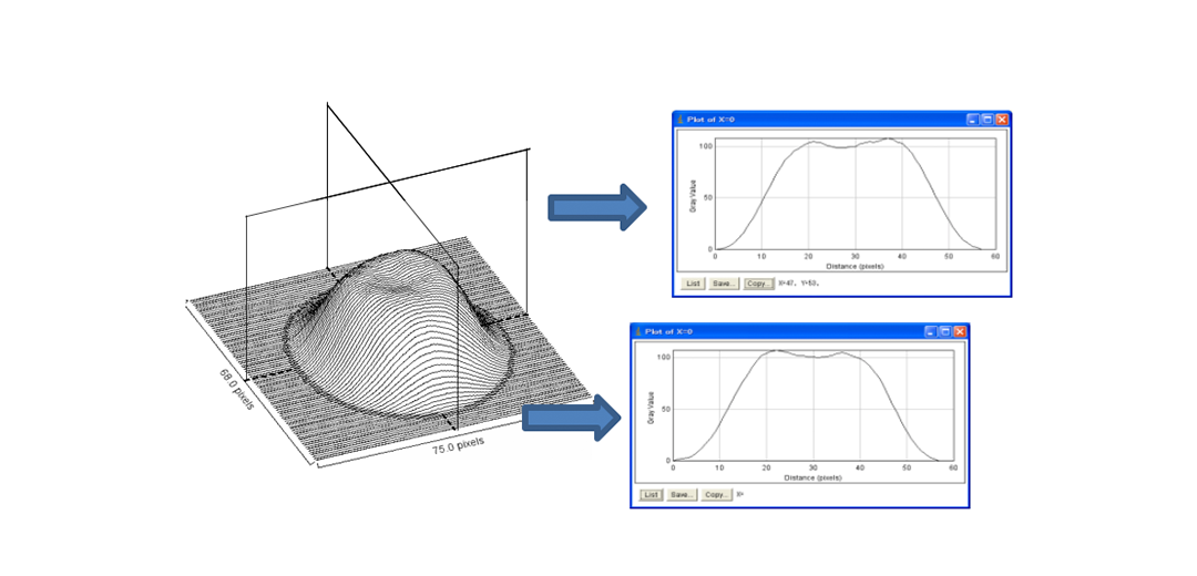
Top hat beam
Ensures excellent in-plane uniformity.
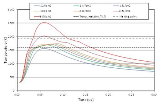
Simulation technology
Optimization of annealing conditions is possible through temperature simulation.
Process atmosphere control Various monitoring functions (beam shape, etc.)
Specification
| Model | SWA-20US | |
|---|---|---|
| Wafer Size | 〜φ200mm (8in) | ◯ |
| Laser | UV-YAG Laser | 10W |
| Beam Size | FWHM | φ100um |
| Process Atmosphere | N2 / Air | |
| Process Temperature | Room Temperature | |
| Wafer Handing | Automatic | |